Quantcast
Channel: Cadence Digital Implementation Blogs

If You Don't See It, You Might Miss It!

$
0
0

The holiday week is here, and while this is a time for relaxing and re-energizing, it's also a perfect opportunity to continue learning and growing. Whether you're a student looking to stay ahead of the curve or a working professional with a thirst for new knowledge, our customer educational training bytes and online courses provide a fun, flexible way to learn during this holiday season.


What Content Is Available in the Digital Design and Signoff Domain?

If you want to explore/understand the complete flow quickly in two days, the Cadence RTL-to-GDSII flow course is for you. To understand how the RTL is synthesized into the gate-level netlist, explore the Genus Synthesis Solution with Stylus Common UI

To learn the detailed implementation flow, from floorplanning to routing, look into this course, Innovus Block Implementation with Stylus Common UI.

Interested in debugging and fixing timing violations with complete signoff techniques? Here is a detailed training course: Tempus Signoff Timing Analysis and Closure with Stylus Common UIAre we sure the complete design works fine after manufacture? How do we keep the design ready for testing? Here are all the fundamentals: Design for Test Fundamentals Training.

How can logic be ensured at every stage of the flow? Can we compare the netlist at each stage? This step is popularly called logic equivalence checking and is related to the course Conformal Equivalence Checking Training.

I have highlighted only a few online courses in this blog, but for more courses on digital design topics, you can look into the learning maps with multiple online courses for each product to get a hands-on experience with labs.

Training Byte References

And don't forget, you can also obtain your Digital Badge after completing many of our training courses.


Becoming Cadence certified with a digital badge puts you ahead by making sure your skills get noticed.

It can help you win new opportunities with customers by showing your qualities and building trust, making you and your projects even more successful. All customers with a valid Cadence Learning and Support account can access the training online 24/7 for free.

If you don’t have a Cadence Support account yet, go to Cadence User Registration and complete the requested information. You can reach out to us at Cadence Training for information on courses, schedules, online training, or live on-site training.

Happy learning!


The Quantum Leap: Equal1 Leverages Cadence Tools for QSoC Design

$
0
0
In today's fast-paced world, the rise of artificial intelligence (AI) is driving skyrocketing expectations for high-performance computing (HPC). To address the expectations, we must overcome complex technical challenges and design and deliver th...(read more)

Digital Design Highlights - New Training Releases, Blogs, Videos and Digital Badges in 2024

$
0
0

 With another year gone, we look back at our most popular blogs from the year and provide a summary of everything else that occurred in the education sector.

In 2024, we published 28more training blogs around Digital Design and Signoff and  proudly presented 1new webinar, if you missed it you can find the recording and  all future webinars we have  planned here.

Some of Our Most Viewed Blogs

Many thanks to all the coworkers who consistently updated their blogs with the most recent, fascinating Training Bytes and training materials. These are links to a few of the most popular blogs.

It’s the Digital Era; Why Not Showcase Your Brand Through a Digital Badge!

Training Insight – Dive into ATPG Flow with Cadence Modus DFT Software Solution 

Did You Miss the RTL-to-GDSII Webinar? No Worries, the Recording Is Available!          

Training Bytes: They May Be Shorter, But the Impact Is Stronger!    

New Training (s) Released in 2024

Genus Physical Synthesis Flow Training

Some of the Most Viewed Training Bytes in Blogs

How to use the Clock Tree Debugger in the Innovus Software

How to Run the Synthesis Without DFT? 

Steps for Multi-Mode Multi-Corner (MMMC) Flow in Genus Synthesis Solution

NewDigital Badges (some examples)

You can also get further information in this blog.

The Training Bytes blog series helped promote some of our Training Bytes, webinars, and scheduled dates for our "Blended" and "Live" trainings. The series also popularized our digital badges. For further information about our trainings, see the Training page and get a complete overview of our  learning map.

We hope that our blog series  helped you address your tasks faster and with ease. If you have any suggestions or desired topics on which you want us to blog, do let us know! 

You can also reach out to us at Cadence Training for information on courses, schedules, online trainings, or live on-site trainings.

RAKs

Please also consider our Rapid Adoption Kits on ASK which are continually updated, here are some recently published RAKs

Here is Some More Interesting News From 2024

We introduced our new online training option  accelerated learning, which will help you to learn Cadence technical content in the fastest, most effective way.

Before starting an accelerated online course, take a pre-quiz to assess current knowledge, skip familiar content, and achieve training goals quickly.

Please find further guidance and explanations in this blog

The accelerated learning option is currently available for the following Digital Design and Signoff online trainings.

We are very proud that we have developed and released our Onboarding Curriculum, especially for new hires, so that they can quickly learn the tools and technologies that will make them productive. Read more in this blog.

  • Cadence Cerebrus tool flow has advanced ML features that can design chips with the best PPA. In 2024, a significant number of customers received badges in the Cadence Cerebrus course.

  • Cerebrus tool flow has advanced ML features that are able to design chips with the best PPA.  More customers have obtained badges on Course on Cerebrus in 2024.

  • All DSG tools are equipped with ML features to enhance efficiency and accelerate semiconductor production.

Cadence Learning and Support: New Courses Section in Content Notification Email

Cadence Learning and Support: Installation and Licensing Help via Chatbot

Please don´t forget to SUBSCRIBE to the Cadence Training Newsletter to receive updates about upcoming training, webinars, and much more. If you have any questions about courses, schedules, online training, blended/virtual live training, or public, or onsite live training, reach out to us at Cadence Training

to the Cadence training newsletter to be updated about upcoming training, webinars, and much more. If you have any questions about courses, schedules, online training, blended/virtual live training, or public, or onsite live training, reach out to us at Cadence Training.

Related Blogs

Training Insights: Cadence Certus Closure Solution Badge Now Available!

Training Insights Accelerated Learning – The more More you You knowKnow, the faster Faster Yyou goGo

If You Don't See It, You Might Miss It!

Need to Reconfigure Your SoC to Meet Functional Safety Standards?

$
0
0

The ISO 26262 standard provides functional safety guidance for semiconductors used in the automotive industry based on the foundational IEC 61508 standard. The Cadence Midas Safety Platform exchanges safety-related information across Cadence tools for a detailed safety analysis and generates a configuration database for your design. The semiconductor vendor does the safety analysis of the fully featured SoC and creates a Midas Safety RC database.

You can use this SoC and embedded software for your application with a modified safety scope, reconfigure the device safety mechanisms, or even add new safety mechanisms. With a vendor-enabled database, you can reassess the safety metrics and create the safety documentation for the reconfigured part.

Check out this video to learn more: Midas Safety Report Creator Introduction

Want to share this and other great Cadence learning opportunities with someone else? Tell them to subscribe.

Hungry for training? Choose the Cadence Training Menu that’s right for you.

Related Courses

Related Blogs

Related Videos

Please see course learning maps for a visual representation of courses and course relationships. Regional course catalogs may be viewed here.

*If you don’t have a Cadence Support account, go to Cadence User Registration and complete the requested information. Or visit Registration Help.

Addressing Sequential Elements Optimization in the VLSI Chip Design

$
0
0

With highly advanced technology, the real designs are getting complex, making the design optimization process complicated and comprising the design results. The sequential cells play a vital role in the chip's optimization and functioning.

Constant, merged, and unused flops, among other factors, impact the chip design's power, performance, and area (PPA) during the synthesis stage. Is there any way to handle the flops optimization for the best PPA results?

The solution lies with the Cadence Genus Synthesis Solution. The ultimate goal of the Genus Synthesis Solution is very simple: deliver the best possible productivity and Power, Performance, and Area (PPA) during register-transfer-level (RTL) logic synthesis of the chip.

 How do you manage the flop optimization?

  • Unused registers on selected modules
  • Disabling sequential merging
  • Optimizing constants on specific flops
  • Preventing register deletion
  • Preventing Selective registers during elaboration
  • Preventing merging of specific flops

Do you want to know how Genus Synthesis Solution manages all these? Explore the videos that cover how to control or enable/disable the optimization of registers or sequential elements in Genus. You can refer to the videos on the ASK Portal (Cadence login required).

Video Links

Removing Unused Registers on Selected Modules in Genus Synthesis Solution (Video)

Preventing Register Deletion in Genus Synthesis Solution (Video)

Disabling Sequential Merging in Genus Synthesis Solution (Video)

Preventing Merging of Specific Flops in Genus Synthesis Solution (Video)

Preserving Selective Registers During Elaboration in Genus Synthesis Solution (Video)

Optimizing Constants On Specific Flops in Genus Synthesis Solution (Video)

Related Resources 

Video Links: Enhance your knowledge of Genus and Joules with short videos

Want to Learn More?

Explore the one-stop solution product pages on the Application Support and Knowledge Portal (Cadence login required).

Related Courses

Want to Enroll in this Course?

We've organized this training for you as "blended" or "Live" training. Please reach out to Cadence Training for further information.

If you want to ensure you are always the first to know about anything new in training, you can use the SUBSCRIBE button on the landing page to sign up for our regular training newsletters.

What's Next?

Grab your Digital Badge after finishing the training and flaunt what expertise you have built up. 😊

Please don't forget to obtain your Digital Badge after completing the training.

Related Blogs

It's the Digital Era; Why Not Showcase Your Brand Through a Digital Badge!

Training Insights – Struggling with Synthesis to Achieve Best PPA Results? - Digital Design - Cadence Blogs - Cadence Community

Unlocking the Concepts of IEEE 1801 Standard for Efficient Power Management - Digital Design - Cadence Blogs - Cadence Community

A Magical World - The Incredible Clock Tree Wizard to Augment Productivity and QoR! - Digital Design - Cadence Blogs - Cadence Community

Static Timing Analysis: Cell Delay vs Cell Drive Strength!

$
0
0

Have you ever wondered how a predator succeeds (or) a prey escapes in the jungle? It’s the breathtaking speed and agility of the predator (say, a leopard🐆 as it chases prey (say, a deer)🦌.

The VLSI circuit operation is very similar. If the driving cell is strong, it takes less delay and changes the output quicker than a weaker driver, which produces a sluggish response and takes longer to produce the same effect at the output pin Q.

Before going into the details, let us know what these terms (cell delay and cell drive strength) mean and why should we take care?

Drive strength and cell delay are two key concepts in digital circuit design, particularly in standard cell libraries used for ASIC and FPGA design. They are closely related and impact timing, power, and area considerations in a design.

Cell Delay

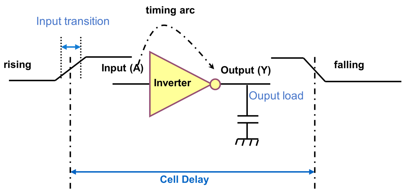
Cell delay refers to the propagation delay of a logic cell, which is the time taken for a change at the input to reflect at the output. It is a function of the input transition time and the effective load at the output pin.

Drive Strength

Drive strength refers to the ability of a logic cell (such as an inverter, buffer, NAND, NOR, etc.) to drive a load. It is usually represented as multiples of a base drive (e.g., X1, X2, X4, X8, etc.), where higher drive strength (X32, X16, etc.) means the cell can provide more current and drive larger loads (longer interconnects, multiple fan-outs). Lower drive strength (X1, X2, etc.) means the cell is weaker and is suitable for driving small loads. As shown in the example below, BUFX2 has lower drive strength, and its delay is higher (high transition time ). BUFX16 has higher drive strength, and its delay is lesser (low transition time).

Relationship Between Drive Strength and Cell Delay

There is an inverse relationship between drive strength and cell delay:
a) Higher drive strength → Lower cell delay: A stronger cell can charge/discharge the output node faster, reducing delay.
b) Lower drive strength → Higher cell delay: A weaker cell takes longer to switch the output due to limited drive current.
However, increasing drive strength comes with trade-offs:
a) Increased area: Higher drive strength cells have larger transistors, which take up more silicon area.
b) Higher power consumption: Larger transistors have higher leakage and dynamic power consumption.

In the below example, you can notice that a higher drive strength cell(BUFX20) has less transition time (0.0349ns), results in less cell delay, and a lower drive strength cell (BUFX2) has a higher transition time (0.1063ns) that results in high cell delay. You can also understand how the area will be affected by different drive strength cells.                              

Choosing the Right Drive Strength

In timing optimization, drive strength selection is a key technique:
a) For high-speed paths, stronger drive strength cells are used to reduce delay.
b) For power-efficient design, weaker drive strength cells are used where speed is not critical.
c) Buffer insertion and sizing: Designers optimize timing by inserting buffers of appropriate drive strengths.

               
Practical Example

Consider a NAND gate with different drive strengths:
- A NAND2_X1 might have a cell delay of 50 ps when driving a small load.
- A NAND2_X8 might have a cell delay of 15 ps for the same load but will consume more power.

Thus, designers must balance drive strength and delay to meet timing constraints while minimizing power and area.

Would you like further details on a specific aspect, such as how EDA tools optimize drive strength?

This Cadence RTL-to- GDSII Flow training course contains the Timing Signoff module that demonstrates the impact of cell delay for different drive strengths for you. Please reach out to Cadence Training for further information.

The course includes slides with audio and downloadable laboratory exercises designed to emphasize the topics covered in the lecture. There is also a Digital Badge available for the training.

You can also access the lab demos created for each course module through a channel video RTL-to-GDSII lab demo videos.

If you want to learn in detail about the Timing Concepts, STA, and Timing Signoff, you can take the following two courses.

Also, the following short training bytes help you understand the concepts quickly, and a few demonstrate how to debug and resolve errors; for more, look here: Training Bytes (Videos)

Training Byte References

Related Blogs

For more information on Cadence's digital design and signoff products and services, visit www.cadence.com.

If you want to receive periodic news and information about Cadence, please sign up and select the topics that interest you.

Happy learning! Thank You.


Conformal AI Studio: Accelerated LEC/ECO/LP with AI/ML-Driven Enhancements

$
0
0

If you're a chip designer or verification engineer, you have likely spent countless hours stressing over whether your design block is functionally accurate; in other words, "Will my chip actually do what it's supposed to?" Today, Cadence is announcing the next evolutions of its Conformal family of products to help you answer that exact question better. Introducing: Conformal AI Studio. I want to take a few words to tell you what inspired the technology, how it works, and why you should care.

The Critical Role of LEC

Logical equivalence checking (LEC) is pivotal in the design implementation process. Traditionally, it allows designers to verify that the functionality remains consistent through various design stages without the need for extensive retesting. By testing the design once at the register transfer level (RTL) and then formally proving that subsequent stages—ranging from gate-level designs to final transistor implementations—are logically equivalent, it not only saves time but also reduces costs significantly. This methodology has long been the backbone of cost-effective verification strategies. However, the last 10 to 15 years have witnessed a paradigm shift in the complexity of designs and the corresponding challenges with LEC.

With SoCs containing 100 times more logic than in previous years and a substantial increase in the number of power domains and functional engineering change orders (ECOs), traditional methods of proving logical equivalence have become increasingly inadequate. The growth of advanced synthesis optimizations, which have proliferated from merely a handful of critical blocks to become a ubiquitous element of the design process, adds to this complexity. Despite these challenges, the fundamental technology underpinning LEC had only seen incremental improvements. As a result, a new approach toward verification is paramount, one that reconsiders the way equivalence is established.

Rethinking Equivalence: A Shift in Approach

To genuinely address the complexities in today's semiconductor designs, the industry must transition from the outdated methodology of proving designs as equivalent in isolation. Real-world designs are not static; they have a life cycle characterized by continuous growth and change. Each stage of a project generates a wealth of historical data that often goes untapped. I would claim that, through most of its history, EDA implementation by default has amnesia. This same inefficiency applies to solutions related to logical equivalence. Our industry must better leverage historical insights to inform and enhance current software solutions.

Embracing AI and ML

One of the most promising avenues for augmenting semiconductor design productivity lies in applying AI and ML techniques. EDA companies, with Cadence at the forefront, are actively deploying these advanced methodologies to streamline chip design and verification processes. AI-driven solutions can vastly improve efficiency by introducing predictive capabilities that draw on historical data. Moreover, AI can assist in optimizing synthesis results by recognizing which optimizations are likely to impact equivalence.

So, given the longstanding value of equivalence checking, the need for a shift in approach, and the broader EDA trends in artificial intelligence and machine learning (AI/ML), what exactly is Cadence announcing today with Conformal AI Studio?

Conformal AI Studio: Core Benefits

Conformal AI is a comprehensive suite that reimagines the current Conformal products and delivers three key new benefits:

  • We're delivering critical productivity improvements that will make users an order of magnitude more efficient. This is possible due to simplified setup and core engine speedups, including a new distributed low-power engine that allows us to scale full chip power signoff to billions of instances. Our new AI-based diagnostic dashboards will streamline usage and enable cross-project insights, while ML-driven abort resolution will help solve one of the most complex problems our advanced users face today.
  • We are introducing a new SmartECO flow that delivers up to 10X better runtime and patch size. We're leveraging earlier RTL-level information and new Boolean optimization algorithms to handle designs with many hierarchies and advanced datapath, while our AI-driven recipe selection makes implementing functional ECOs simple and efficient.
  • While the Conformal family is committed to always being implementation tool agnostic, we're doubling down on ensuring our flows work best with our Cadence tools. New support for sequential optimizations in the Cadence Genus, Joules, and Innovus solutions, as well as expanded reinforcement learning techniques, can help both lower power and improve performance.

Conformal AI Studio: AI/ML Innovations

In addition to these critical new core engines and flow improvements, this generation of Conformal technology leverages AI/ML in a number of new ways. Deep integrations to Cadence's JedAI big data platform allow design teams to mine data across a project's history and learn from customers' unique design styles and tool strategies. Conformal AI Studio can now intelligently spawn off multiple parallel scenarios using the Cadence Cerebrus reinforcement learning system to rapidly explore the full solution spaces for the most challenging problems, like proving equivalence when facing complex aborts or ensuring ECO patches are both functionally optimal and implementable through place-and-route, STA, and physical signoff.

Conformal AI Studio: Always Implementation Agnostic

For decades, the Conformal family has been the industry leader in the LEC subset of formal verification and is the key auditor for ensuring that digital implementation tools from both Cadence and other EDA vendors do what they're supposed to. We have never wavered from that mission of being your trusted golden signoff regardless of your implementation flow, and the Cadence Conformal AI Studio represents the exciting next chapter.

Conformal AI Studio: New Product Offerings

Taken together, these Conformal AI Studio innovations will help your implementation teams achieve their design goals and are available from three core products:

  • Conformal AI Equivalence– Enables distributed Boolean LEC, AI dashboards, and ML-driven proof engines
  • Conformal AI ECO– Automates pre- and post-mask functional ECO generation, creating high-quality, efficient, and implementable patches that ensure schedule predictability
  • Conformal AI Low Power– Verifies that low-power circuit structures in complex SoCs match the design's power intent using distributed and hierarchical flows and performs efficient two-design low-power compare

Conclusion

As the semiconductor industry grapples with soaring design complexities, harnessing innovative technologies becomes increasingly urgent. LEC remains a cornerstone of verification practices, but its evolution is necessary to meet contemporary challenges. By embracing the capabilities of AI and ML, we can help you turn data into actionable insights, optimize workflows, and foster collaboration across teams. This is not just about keeping pace; it's about leading the charge toward a future where engineers can design smarter, faster, and more efficiently than ever before. The transformation is underway, and Cadence can help chip designs confidently answer that overarching question of "Will my chip do what it's supposed to?" with "Yes, it will, when you sign off with Conformal AI Studio!"

Learn more about Conformal AI Studio.

The Power of Less is More! Minimize Power, Maximize Chip's Efficiency!

$
0
0

Optimizing power can be a very convoluted and crucial process. To make design chips meet throughput goals and optimal power consumption, you need to plan right from the beginning! Power is HOT and touches everything and everybody!

Low-power synthesis is one of the important stages in the full IC flow. Using various techniques, you synthesize the design from behavioral description to gates while optimizing for dynamic and leakage power. Do you want to use multiple supply voltage (MSV) design, power shutoff (PSO) synthesis, dynamic voltage frequency scaling (DVFS), or other techniques to optimize your power results?

But stuck as you are new to the low-power world, do the various power terminologies look like a complicated maze for you?

  1. Power domains
  2. Power intent
  3. Power modes
  4. Level shifter
  5. Isolation logic
  6. State retention power gating
  7. Gate-level dynamic power optimization
  8. Clock gating
  9. Multiple threshold voltage
  10. Power shutoff
  11. Dynamic voltage frequency scaling
  12. Glitch

The list goes on…

Wondering how to enhance your knowledge of these concepts to ensure proper planning for low-power optimization? Gear up! You don't need too many resources to elevate your proficiency.

We believe disseminating the knowledge amplifies its power. We want you to leverage our vast resources to develop expertise and knowledge of various chip design concepts and flows. The magic lies in your pocket! Unlock your mobile and start relaxing with YouTube videos!

Er…don't get confused! The Cadence YouTube channel hosts a Customer Education Training Bytes channel. This provides a video repository of short conceptual videos on YouTube. The learning is just a click away! Click the links below to explore the basic low-power terminologies and more!

What Are Power Domains

What Is Power Intent

What are Power modes

What Is a Level Shifter

What Is an Isolation Logic

What Is State Retention Power Gating

How to do Gate Level Dynamic Power Optimization

How to Optimize Dynamic Power

What is Clock Gating and How to Reduce Clock Power

Understanding Multiple Threshold Voltage Optimization

What Are Multiple Supply Voltage and Power Shutoff Methodologies?

What Is Dynamic Voltage Frequency Scaling

What Is a Glitch

 As a next step, you can further leverage the vast database of videos and detailed training on Cadence Application Support and Knowledge Portal (Cadence login required).

Related Resources

Video Links: Enhance your knowledge of Genus and Joules with short videos

Want to Learn More?

Explore the one-stop solution product pages on Cadence Application Support and Knowledge Portal (Cadence login required).

Related Courses

Want to Enroll in this Course?

We organize this training for you as "Blended" or "Live" training. Please reach out to Cadence Training for further information.

Please don't forget to obtain your Digital Badge after completing the training.

If you want to ensure you are always the first to know about anything new in training, then you can use the SUBSCRIBE button on the landing page to sign up for our regular training newsletters.

Related Blogs

If You Don't See It, You Might Miss It! - Digital Design - Cadence Blogs - Cadence Community

Get Noticed! With a Digital Badge from Cadence Training

Digital Design Highlights - New Training Releases, Blogs, Videos and Digital Badges in 2024 - Digital Design - Cadence Blogs - Cadence Community

Addressing Sequential Elements Optimization in the VLSI Chip Design - Digital Design - Cadence Blogs - Cadence Community

A Magical World - The Incredible Clock Tree Wizard to Augment Productivity and QoR! - Digital Design - Cadence Blogs - Cadence Community


Spaghetti Is Great! Spaghetti Code? Not So Much

$
0
0

Have you ever found yourself in an Italian restaurant, twirling your fork around a plate of delicious spaghetti? Good spaghetti is a true gift, but spaghetti code? Not so much.

Spaghetti code refers to complex, tangled programming code that is a nightmare to follow and maintain. We've all been there when we have inherited code from someone who has moved on, and it's now our job to maintain it or debug it in a crisis.

Just like a plate of spaghetti where every strand is intertwined, spaghetti code's intricacies can make a programmer's job unnecessarily complicated.

Here's why simple programming commands are preferred over complex ones and how embracing simplicity can save your sanity—and time.

Simple code is like a straight road—it efficiently gets you from point A to point B. It's easy to read, debug, and maintain. When you write simple code, you're doing yourself a favor and helping anyone who might have to deal with your code in the future. It's like leaving clear signposts for fellow travelers, ensuring that no one gets lost in a maze of convoluted instructions.

On the other hand, complex code is the equivalent of sending someone on a detour through a dense forest with a vague map. They might eventually find their way, but not without frustration and wasted time. Keeping your code simple ensures that the journey is smooth and straightforward.

A Simple TCL Example

Here's a basic example of a TCL script that reverses a string:

set str "Hello, World!"

set reversed_str [string reverse $str]

puts $reversed_str

This script uses the set command to define a string variable str. The string reverse command reverses the string, and the puts command prints the reversed string to the console. It's straightforward to understand.

A More Complex TCL Example

Now, let's look at a more convoluted TCL script that performs the same task but involves multiple steps and additional logic:

set str "Hello, World!"

set len [string length $str]

set reversed_str""

for {set i [expr $len - 1]} {$i >= 0} {incr i -1} {

}

}

puts $reversed_str

In this script, we first define the string variable str and calculate its length using the string length command. We initialize an empty string reversed_str. The for loop iterates over each character in the string from the end to the beginning, and the append command adds each character to the reversed_str. Finally, the puts command prints the reversed string to the console.

I think that we would all agree that, wherever possible, simplicity is preferred to needless complexity.

In the spirit of simplicity, I have created some videos showing some simple and useful commands in Innovus Implementation System Stylus Common UI.

Useful Commands to Get Design Information in Innovus Stylus Common UI Software (Video)

Useful General Purpose and Unix Commands used with Innovus Stylus Common UI Software (Video)

In the end, spaghetti has its place on your dinner table, not in your code. So, next time you're tempted to write that complex command, remember that a simple approach can save you time, effort, and a lot of headaches.

Related Resources

Innovus Block Implementation with Stylus Common UI Training Course

Tcl Scripting for EDA Training Course

Tcl Scripting for EDA + Intro to Tk Training Course

You might also be interested in the Learning Map, which guides you through recommended course flows as well as tool experience and knowledge-level training modules.

Find out how to get an account on the Cadence Learning and Support portal.

SUBSCRIBE to the Cadence training newsletter to be updated about upcoming training, webinars, and much more. If you have any questions about courses, schedules, online training, blended/virtual live training, or public or onsite live training, reach out to us at Cadence Training.

Happy Coding!

Silicon Skylines: Crafting the Future of Electronics

$
0
0

The world of Electronic Design Automation (EDA) is fascinating, where we transform humble grains of sand into sophisticated silicon chips that power our modern lives. Imagine this journey as a grand adventure, akin to building a bustling city from scratch. Buckle up as we take you through the highlights of our latest course, "Introduction to Electronic Design Automation.

Imagine standing on a beach surrounded by endless grains of sand. Little do you know, these tiny particles hold the potential to become the foundation of cutting-edge technology.

The World of Semiconductors Is Like Building a City

Just as a city planner needs various maps and models to design a well-functioning city, chip designers require different views and models to create a successful IC.

Then comes the magic of EDA, which turns ideas into reality. They help designers automate the complex chip design process, from initial concept to final tape-out. Think of EDA as the city's primary architect, orchestrating every detail to ensure the final product is nothing short of perfection. And just like a city, a chip must be meticulously planned, verified, and tested before it can come to life.

Do You Think Designing a Chip Is Easy as a City Planner?

Of course, no journey is complete without challenges! Imagine city planners dealing with the same challenges as chip designers. "Oops, we forgot to connect the power grid to the new neighborhood. Let's reroute the entire city's electricity!" Or, "We need to fit 10 more skyscrapers into this block without increasing the land area. No problem, we'll stack them vertically!"

As we continue to push the boundaries of technology, the role of EDA in shaping the future of electronics becomes ever more critical. From autonomous vehicles to smart cities, the possibilities are endless. So, the next time you use your smartphone or marvel at a self-driving car, remember the incredible journey from sand to Silicon City that made it all possible.

Want to Explore How Sand to Silicon Gives Birth to a Chip?

Don't worry! We have a solution in the form of comprehensive training. Stop by for this short course to unveil the magic of electronic design automation in building the semiconductor world.

Course Title: Introduction to Electronic Design Automation Training Course | Cadence

This course introduces Electronic Design Automation (EDA), which is vital in advancing integrated circuit design and development. In this course, you will learn EDA's critical components and technologies in creating a product from "sand to silicon to system." You will identify major electronics industry challenges and solutions Cadence offers. The course also includes an overview of the digital twin concept and insights into using EDA tools in our supply chain for product development. You will also identify hardware security gaps, outline the solution, and explore the semiconductor system and end markets.

Please note an accelerated learning path is also available for this training.

What's Next?

Grab your Digital Badge after finishing the training and flaunt what expertise you have built up. 

Want to Enroll in this Course?

We've organized this training for you as a "Blended" or "Live" training. Please reach out to Cadence Training for further information. If you want to ensure you are always the first to know about anything new in training, you can use the SUBSCRIBE button on the landing page to sign up for our regular training newsletters.

As a next step, you can further leverage the vast database of videos and detailed training on Cadence Application Support and Knowledge Portal (Cadence login required).

Related Resources 

Video Links: Enhance your knowledge of Digital flow with short videos at the ASK portal:

Want to Learn More?

Explore the one-stop solution product pages on Cadence Application Support and Knowledge Portal (Cadence login required). Enroll in the Digital IC design fundamental course: Digital IC Design Fundamentals Training Course | Cadence

Did You Know?

The Cadence YouTube channel hosts a Customer Education Training Bytes channelHere, you can view a variety of training bytes for which you do not need a Cadence ASK account.

Related Blogs

Get Noticed! With a Digital Badge from Cadence Training

The Power of Less is More! Minimize Power, Maximize Chip's Efficiency! - Digital Design - Cadence Blogs - Cadence Community

Digital Design Highlights - New Training Releases, Blogs, Videos and Digital Badges in 2024 - Digital Design - Cadence Blogs - Cadence Community

Unlocking the Concepts of IEEE 1801 Standard for Efficient Power Management - Digital Design - Cadence Blogs - Cadence Community

Microlearning: The Snackable Knowledge Training Videos

$
0
0

Are you looking to level up your digital design skills—one byte at a time? Ohoo! I am supposed to ask this question at the end of this blog.

Ever feel like your brain is a sponge that’s just not soaking up enough? Or maybe you have tried to learn something new and ended up feeling like a cat chasing a laser pointer—excited but ultimately confused? Fear not, my friend! Microlearning is here to save the day, and it’s as fun as a barrel of monkeys. Let’s dive into this quirky world where learning is bite-sized and engaging.

Welcome to the world of microlearning, where education is as bite-sized as your favorite snacks and just as satisfying! Imagine learning as a series of delightful appetizers rather than a daunting seven-course meal. Intrigued? Hungry? Let's dive into the deliciously funny world of microlearning!


What Is Microlearning?

Microlearning is like the tapas of the educational world—small, tasty morsels of knowledge that you can savor anytime, anywhere. It's the perfect solution for those of us with the attention span of a goldfish and the schedule of a busy bee. Think of it as the ultimate brain snack!

Think of it as a snackable learning experience—quick, powerful, and easy to digest. No fluff, no filler—just the essential tips, tricks, and techniques you need to transform your designs from meh to mind-blowing.

Why Microlearning Works?

Snack-sized portions: Just like you wouldn't eat a whole cake in one sitting (well, most of us wouldn't), microlearning breaks down information into manageable chunks. It's like having a bite of knowledge without the brain freeze.

Example: What if you had five minutes to learning about a new piece of technology?

On-the-go goodness: Whether you're waiting for your coffee to brew or pretending to listen in a meeting, microlearning fits into those tiny pockets of time. It's like sneaking in a quick snack without anyone noticing.

Example: Discover the following demo videos created on implementation topics.

Imagine learning a new skill in the time it takes to microwave popcorn with short videos or enjoying fun, colorful infographics packed with info. Flashcards are perfect for quick, essential knowledge, while quizzes offer a bit of friendly competition. Tune into bite-sized demo videos.

Final Thoughts

Microlearning is more than just a trend—it's a powerful tool that adapts to the needs of modern learners. By embracing this approach, you can enhance your knowledge, boost your productivity, and stay ahead in an ever-evolving world. So, why not try microlearning and unlock your full potential?

If you are looking for one-minute videos, below are the references to learn about the definitions of the full Digital Design Flow (RTL-to-GDSII Flow).

These training bytes below are available on Cadence Support and YouTube.

If you want to dive into the detailed steps of Cadence RTL-to-GDSII Flow, there are lab demo videos in this channel, by which are also bite-sized videos. Also, you can learn from this 45-minute webinar that covers the complete flow. Did You Miss the RTL-to-GDSII Webinar? No Worries, the Recording Is Available!

TheCadence RTL-to-GDSII Flow [Online Course] training is also available as both"Blended" and"Live" Please reach out to Cadence Training for further information.

And don't forget to obtain your Digital Badge after completing the training!

Microlearning is the ultimate brain snack that fits into your busy life. It's fun, engaging, and oh-so-satisfying. So, why not try microlearning and munch your way to knowledge? As a best practice, for more updated content like this, you can read quick blogs in the Cadence Community and get daily knowledge from email updates by SUBSCRIBING to the Cadence training newsletter to be updated about upcoming training, webinars, and much more, and you can explore ask.cadence.com to get support anytime!

Related Blogs

Related Training Bytes

Semiconductors: Pioneering Extraordinary Growth in the 20th Century

$
0
0

Semiconductors have revolutionized the world, powering everything from smartphones to space shuttles. But how did this incredible journey begin, and where is it headed? Welcome to Semiconductor 101 training, where we explore the fascinating evolution of semiconductor technology and its impact on our lives.

This course will introduce you to where semiconductors started and give you insights into where the semiconductor industry is now.

What Is EDA?

Do you have the answer to this question? Here is it.

Electronic Design Automation (EDA) software is essential for designing semiconductor chips, and Cadence stands out as a leader in this industry. Cadence offers a comprehensive suite of EDA tools that support the entire chip design process, ensuring efficiency and innovation.

In addition to EDA tools, Cadence has a significant presence in the Intellectual Property (IP) market. IP refers to predesigned chip components that designers can integrate into their chip designs, streamlining development and reducing time-to-market.

A key driver of the semiconductor industry’s growth has been Moore’s Law, which has accurately predicted the exponential increase in chip complexity and performance over the years. This principle continues to guide advancements in chip design, shaping the future of technology.

Semiconductor technology has evolved significantly, starting from 3 µm and advancing to 3 nm today. This journey includes innovations in structure, transitioning from planar MOSFET to FinFET and then to GAAFET. As technology scales down, the complexity and the number of transistors within a chip increase, enhancing performance and functionality.

Is Chip Design Easy or Not?

A significant thing to consider is whether chip design is a complex process.

It is a time-critical one. Over time, semiconductor industries have changed their priorities in chip design from Area (A) to Performance (P) and then Power (P), but now they focus on all (PPA) at a time.

Cadence's Role in Chip Design

Cadence EDA tools play a crucial role in the chip design process, enabling the creation of chips with superior Power, Performance, and Area (PPA). These tools are essential for achieving high-quality designs that meet the demanding requirements of modern technology.

Most Cadence Tools have built-in AI features, enhancing the PPA with faster Turn-Around Time (TAT).

The Evolution of ICs: Embracing Multi-Die Integration

In the past, integrated circuits (ICs) primarily featured a single die. Today, the industry has shifted towards heterogeneous integration, combining multiple dies with various logic types. This innovation has led to advanced packaging techniques utilizing 2D, 2.5D, and 3D IC integration methods. These methods enable the creation of more complex chips with higher transistor counts and greater density, paving the way for enhanced performance and functionality.

Cadence offers a comprehensive suite of tools for 3D IC design, enabling efficient planning, implementation, and analysis of multi-die systems.

Cadence PCB tools improve the packaging of the IC and assembly in the PCB to create a system for any application.

System Platforms

Software development and testing are made easy with the Cadence emulation platforms, which significantly helps software developers.

FPGA is used to prototype designs before chip fabrication. This way of prototyping greatly helps hardware designers validate their design functionality in a hardware environment. The Cadence FPGA prototyping system validates complex designs.

Semiconductor Customer Markets

Who are the current prominent semiconductor customer markets? What is their focus on?

Semiconductors play a significant role in many industries, such as consumer, hyper-scale, mobile, communication, automotive, aerospace/defense, health, etc.

The world of electronics is booming with innovation, transforming industries and everyday life. With around 1.5 billion mobile phones shipped annually, the mobile sector is a giant in the semiconductor market. Meanwhile, the automotive industry is witnessing a surge in electronic integration, driving advancements and shaping the future of transportation. Embrace the rise of semiconductors and be part of this exciting journey!

Cadence Intelligent System Design strategy transforms the chip design process, significantly advancing across multiple fields.

This strategy stands strong regarding design excellence, system innovation, and pervasive intelligence. With these core principles, Cadence delivers comprehensive customer support in chip design through its cutting-edge EDA software and IP.

The semiconductor industry has come a long way, driven by relentless innovation and technological advancements. As we look to the future, the possibilities are endless.

To dive deeper into this exciting field, enroll in our Semiconductor 101 training course and take an exam to earn your Digital Badge, as shown below, to showcase your expertise.

To learn about other courses, see the Learning Map and take training courses in different areas of chip design based on your interests.

Related Courses

Digital IC Design Fundamentals

Cadence RTL-to-GDSII Flow Training

SystemVerilog for Design and Verification

To receive Cadence Training-related news and events, sign up using this link.

*If you don’t have a Cadence support account, go to Cadence User Registration and complete the requested information. Or visit Registration Help.

Transforming Chip Design with Cadence Cerebrus AI Studio

$
0
0

Cadence Cerebrus AI Studio

Cadence is transforming chip design with the launch of Cadence Cerebrus® AI Studio, the industry's first agentic AI, multi-block, multi-user design platform. This cutting-edge solution accelerates system-on-chip (SoC) design by 5 – 10X while achieving unparalleled power, performance, and area (PPA) gains. Built to empower engineers with intelligent workflows and advanced data analytics, Cadence Cerebrus AI Studio represents a transformative shift in semiconductor design.

Learn more about this breakthrough technology in the news story: Transforming Chip Design with Agentic AI: Introducing Cadence Cerebrus AI Studio.

Early Customer Success Stories

Companies like Samsung and STMicroelectronics are already seeing remarkable results from Cadence Cerebrus AI Studio. These organizations have reported significant improvements in productivity, reduced turnaround times, and optimized PPA outcomes.

SSIR

By leveraging Cadence Cerebrus AI Studio, Samsung Semiconductor India Research (SSIR) achieved an 8 – 11% PPA improvement on advanced subsystems, alongside faster design convergence using features like advanced data analytics, live design dashboards, and smart model replay.

Samsung Semiconductor India Research Leverages Cadence Cerebrus AI Studio

Watch the SSIR Success Story

SARC

At Samsung Austin Research and Development Center (SARC), engineers experienced a 4X boost in productivity with enhanced hierarchical design methodologies, smart workstreams, and a customizable live design dashboard.

SARC Endorses Cadence Cerebrus AI Studio

Watch the SARC Success Story

Why Choose Cadence Cerebrus AI Studio

Key features of Cadence Cerebrus AI Studio include:

  • Multi-block, multi-user infrastructure for increased productivity
  • Agentic AI hierarchical SoC design optimization
  • Live customizable design dashboard for seamless collaboration
  • Intelligent workflows for fastest time to design targets
  • AI-driven advanced data analytics for identifying bottlenecks

Whether you're optimizing designs for high-performance computing, automotive applications, or cutting-edge physical AI solutions, Cadence Cerebrus AI Studio ensures your team performs at its best while meeting aggressive design targets.

Be Part of the Next Wave of Chip Design

Elevate your team's productivity with agentic AI workflows and stay ahead of the curve with Cadence Cerebrus AI Studio. Discover more about this game-changing platform: Cadence Cerebrus AI Studio Product Page.

Elevate Your EDA Skills: Achieve Unmatched PPA with Genus Synthesis Solution

$
0
0

As the electronic design automation (EDA) landscape continues to evolve, the importance of efficient and effective synthesis has grown exponentially. With the increasing complexity of modern system-on-chips (SoCs), design teams face significant challenges in achieving optimal power, performance, and area (PPA) results. In this context, the Cadence Genus Synthesis Solution has emerged as a game-changer, helping designers overcome the hurdles of RTL logic synthesis. However, to unlock the full potential of this powerful tool, it's essential to develop expertise in Genus synthesis techniques.

The Synthesis Challenge

Design synthesis can be daunting, especially when working with complex designs. Designers typically encounter issues such as PPA limitations, timing constraints, and area optimization. These challenges can slow down the design process and impact overall productivity. To overcome these obstacles, design teams require in-depth knowledge of synthesis best practices and the ability to debug common problems.

Bridging the Knowledge Gap with Cadence Genus Synthesis Solution Training

To address this challenge, Cadence offers comprehensive training on the Genus Synthesis Solution:

  1. Genus Synthesis Solution with Stylus Common UI

Discover the capabilities of Cadence Genus Synthesis Solution with Stylus Common UI and how it addresses the SoC design productivity gap.

This training provides a solid foundation for the Cadence Genus Synthesis Solution, covering design constraining, static timing analysis, datapath logic evaluation, physical synthesis, low-power optimization, scan insertion, interfacing with LEC, and other Cadence tools.

By the end of the training, you can run a comprehensive synthesis flow on a design with specific requirements, resulting in optimized area, timing, and power consumption.

  1. Advanced Synthesis with Genus Synthesis Solution

Elevate your skills with advanced synthesis techniques to optimize PPA results and ensure alignment with place and route processes. The training guides debugging issues in complex design synthesis, focusing on timing, area, and power optimization. It includes example problem scenarios commonly encountered in synthesis flows and offers strategies for effective debugging.

Hands-on Learning with Labs and Training Bytes

To reinforce theoretical knowledge, the training includes:

Labs: To facilitate a seamless learning experience, we provide hands-on labs encompassing various design scenarios.

The training and lab exercises are specifically designed to help you reach your objectives, with step-by-step lab instructions conveniently available in the interactive lab book.

Lab Videos: Here's where it gets exciting!"

We provide dynamic video content for each training lab to support your learning journey. Every lab module includes a demo-style walkthrough of the instructions, making it easier to ramp up the tools and troubleshoot any steps. Whether you're just a beginner in synthesis or already have some experience, we're here to help you navigate it confidently.

Kickstart your journey to becoming a synthesis expert with our captivating series of short lab videos, now available on the ASK site.

How to Run the Setup for Synthesis, Load Libraries, and Design And Elaborate The Design Module in Genus Synthesis Solution? (Video)

Demo: Analyze, Synthesize, and Optimize the design for the best possible timing with the Genus Synthesis Solution (Video)

By investing in Cadence Genus Synthesis Solution training, design teams can unlock the full potential of this powerful tool, achieving best-in-class PPA results and accelerating their EDA innovation journey.

 Online Class: Get ready for the most thrilling experience with Accelerated Learning!


The more you know, the faster you go!

Grab the cycle       or hike    it based on your existing knowledge.

Take the quiz and increase your learning pace!!


What's Next?

Grab your  Digital Badge after finishing the training and flaunt the expertise you have built up. 

Want to Enroll in this Course?

We organize this training for you as a "Blended" or "Live" training. Please reach out to Cadence Training for further information. If you want to ensure you are always the first to know about anything new in training, you can use the SUBSCRIBE button on the landing page to sign up for our regular training newsletters.

As a next step, you can further leverage the vast database of videos and detailed training on Cadence Application Support and Knowledge Portal (Cadence login required).

Short Training Bytes/videos:

Enhance the Genus Synthesis Solution experience with short videos: Genus Synthesis Solution: Video Library

Did you know?

The Cadence YouTube channel hosts a Customer Education Training Bytes channel

Here, you can view a variety of training bytes for which you do not need a Cadence ASK account.

Related Blogs:

Recording Now Available: Intro to Genus iSpatial Synthesis Flow Webinar - Digital Design - Cadence

Get Noticed! With a Digital Badge from Cadence Training

The Power of Less is More! Minimize Power, Maximize Chip's Efficiency! - Digital Design - Cadence Blogs - Cadence Community

Digital Design Highlights - New Training Releases, Blogs, Videos and Digital Badges in 2024 - Digital Design - Cadence Blogs - Cadence Community

Unlocking the Concepts of IEEE 1801 Standard for Efficient Power Management - Digital Design - Cadence Blogs - Cadence Community

From Chaos to Clarity: Mastering PBS MiM Flow Without the Land Disputes

$
0
0

Let's face it—when most of us hear "partition," we think of land disputes, family feuds, or that one cousin who insists on measuring every square inch of their share.

However, in the world of chip design, partition-based synthesis (PBS) is less about drama and more about design harmony.

Ever feel like you're stuck in a loop, optimizing the same logic block over and over—like déjà vu with a side of synthesis fatigue? Imagine you could optimize something once and just copy-paste the brilliance everywhere!

PBS MiM (multiple instantiated modules) breaks that cycle. Instead of re-optimizing each N module instance individually (and slowly losing your will to debug), it optimizes the logic once and smartly replicates the result across all instances. It's like telling your tool, "Learn it once, apply it everywhere." The result? Faster runtime, less redundancy!

In the fast-evolving world of SoC design, efficiency, scalability, and performance are non-negotiable. That's where the PBS MiM Flow in the Genus Synthesis Solution comes into play—empowering design teams to handle complex hierarchical designs easily and precisely.

To help you learn this magical and powerful methodology, we've curated a series of insightful videos now available on the ASK portal:

1. What Is PBS Multiple Instantiated Modules (MiM) Flow? (Video): Think of this as your "Partitioning 101"—minus the land lawyers. This video introduces the concept of PBS MiM flow, explaining how it helps you manage large, hierarchical designs without losing the synthesis quality. While partitioning land can lead to chaos, partitioning your design with PBS MiM actually reduces complexity and improves turnaround time. Who knew?

2. Understanding PBS Multiple Instantiated Modules (MiM) Flow in Genus Synthesis Solution (Video): Through this video, take a deeper dive into how the MiM flow is implemented within the Genus Synthesis Solution environment. The session walks you through how Genus handles MiM flow—like a pro chef slicing and dicing a complex recipe into manageable, reusable chunks. This video highlights how MiM facilitates improved reuse and quicker turnaround times in large-scale designs.

3. How to Control PBS MiM (Multiple Instantiated Modules) Flow in Genus Synthesis Solution (Video): Learn how to fine-tune your MiM flow and manage instantiations. This video provides practical guidance on controlling and customizing the MiM flow.

Whether you're an experienced synthesis engineer or just beginning to explore hierarchical design methodologies, these videos are a must-watch. Head over to the ASK portal before your next synthesis run and start exploring today!

Why You Should Watch These Videos?

 Accelerate your synthesis flow with smarter reuse and modularity.

🖐 Say goodbye to repetitive grunt work—MiM handles it like a champ.

📈 Boost your TAT while keeping synthesis coherence intact.

So, next time someone says "partition," don't think of land. Think logic. Think PBS MiM!

What Else Can You Explore at ASK Portal?

Check out these newly added Genus Synthesis Solution videos:

What Is Nested Interface Logic Model (ILM) Flow?

How to Control Datapath Optimization in Genus Synthesis Solution?

How to Write the Timing Model in Genus Synthesis Solution?

How to Report Clock Gating History in Genus Synthesis Solution?

How to Report Ungroup Modules in Genus Synthesis Solution?

How to Report Clock Gate Declone in Genus Synthesis Solution?

Watch Free Online Trainings

The Online Trainings are free for all Cadence customers with a Cadence ASK Account. For "Live" or "Blended" instructor-led training sessions, please contact Cadence Training.

Further enhance the Genus Synthesis Solution learning experience with short videos: Genus Synthesis Solution: Video Library.

Did You Already Know?

The Cadence YouTube channel hosts a Customer Education Training Bytes channel.

Here, you can view a variety of training bytes for which you do not need a Cadence ASK account.

Related Blogs

Get Noticed! With a Digital Badge from Cadence Training

The Power of Less is More! Minimize Power, Maximize Chip's Efficiency!

Digital Design Highlights - New Training Releases, Blogs, Videos and Digital Badges in 2024

Unlocking the Concepts of IEEE 1801 Standard for Efficient Power Management